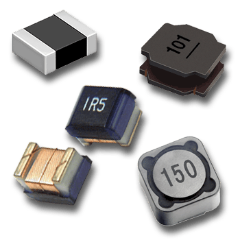
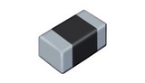
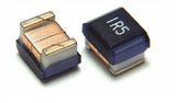
CHIP INDUCTOR
 VHF - CHIP HIGH FREQUENCY INDUCTOR
- High self-resonant frequency.
- Multilayer monolithic construction yields high reliability
- Excellent solderability and heat resistance for either wave or reflow soldering.
CMI - FERRITE CHIP INDUCTOR
- Miniature volume.
- No cross coupling between inductors due to low magnetic shield and high reliability.
- No lead, ideal for high density SMT installation, with no directionality.
- Superior solderability and resistance to soldering heat, ldeal for wave or reflow soldering.
CMP - HIGH CURRENT FERRITE CHIP INDUCTOR
- High rated current and low direct-current resistance.
- No cross coupling between inductors due to low magnetic sheild and high reliability.
- No leads, ideal for high density SMT installation with no directionality.
- Superior solderability and resistance to soldering heat, ideal for wave or reflow soldering
 CBG - FERRITE CHIP BEADS (General)
- Under the same size the multilayer chip beads produce higher impedance than plug-in beads.
- These CBG series have substantial EMI & RFI suppression by simply mounting them onto PCB
- Suitable EIA standard in shape and dimension of chip beads; Can be mounted automatically by SMT equipments.
CBW - FERRITE CHIP BEAD (High Current)
- These CBG series have substantial EMI & RFI suppression by simply mounting them onto PCB
- Suitable EIA standard in shape and dimension of chip beads; Can be mounted automatically by SMT equipments.
CBM - FERRITE CHIP BEAD (Ultra High Current)
- A unique terminal electrode structure ensures ensures permissible current 6.0A (max).
- High impedance and EMI suppression effective over a wide frequency range.
- Suitable reflow and wave soldering.
CBH - FERRITE CHIP BEAD (Low Frequency High Resistance)
- CBH series beads exhibit high resistance at low frequency, which makes it stop the reduction of the wave-form
effectively.
CBY - FERRITE CHIP BEAD (High Impedance)
- Excellent solderability and high heat resistance for either reflow or wave soldering.
- No leads, ideal for SMT.
- Monotilithic inorganic material construction for high reliability.
FHW - WIRE WOUND CHIP CERAMIC INDUCTOR
- Minature size, suitable for SMT.
- Using terminal electrode structure to restrain the parasitic component effect quite caused by lead.
- High Q value and precise inductance tolerance.
- Execellent in solderability and heat resistance.
FHW - WIRE WOUND CHIP FERRITE INDUCTOR
- Minature size, suitable for SMT.
- Using terminal electrode structure to restrain the parasitic component effect quite caused by lead.
- Low DC resistance, high current and high inductance.
- Execellent in solderability and heat resistance